
Research team creates process to grow sub-nanometer transistors:
A South Korean research team led by Director Jo Moon-Ho of the Center for Van der Waals Quantum ...
techspot.com/news/103696-research-team-creates-process-grow-sub-nanometer-transistors.html

Story Details
| Last Updated | |
| Total Articles | 1 |
Main Topics

factory where devices such as integrated circuits are manufactured

crystalline materials consisting of a single layer of atoms

Similar to This
Previous

Single 2D crystal transforms into transistor with built-in insulation and electrical contacts
phys.org/news/2026-10-2d-crystal-transistor-built-insulation.html

Scientists just measured the smallest possible contacts for future computer chips
phys.org/news/2026-07-scientists-smallest-contacts-future-chips.html


NSRAM: The Artificial Neuron on a Silicon Chip: The result is a simple and efficient neuromorphic device that mimics a brain cell
spectrum.ieee.org/artificial-neurons-on-silicon-chips


techxplore.com Jun 26
Dog-bone design helps 2D nanoribbon transistors stay fast and efficient as widths shrink
techxplore.com/news/2026-06-dog-bone-2d-nanoribbon-transistors.html


Nature Jun 01
Monolithic three-dimensional integration of silicon transistors: Monolithic, three-dimensional (3D) integrated circuits promise advantages in packing density ...
nature.com/articles/s41586-026-10496-6

Most lab testing quietly inflates 2D transistor performance, research reveals: For nearly two decades, two-dimensional (2D) semiconductors have been studied as a ...
phys.org/news/2026-02-lab-quietly-inflates-2d-transistor.html


Intel details progress on fabbing 2D transistors a few atoms thick in standard high volume fab production environment — chipmaker outlines 300-mm fab ...
tomshardware.com/tech-industry/semiconductors/intel-shows-300-mm-fab-compatible-integration-of-2d-transistor-contacts-and-gate-stacks

First truly 3D chip fabbed at US foundry, features carbon nanotube transistors and RAM on a single die — future devices could have up to 1000x improvement in ...
tomshardware.com/tech-industry/semiconductors/stanford-led-team-builds-3d-ai-chip-at-us-foundry-reports-4x-performance-gains

dlvr.it Oct 12 25
Inside the belly of the beast: A technical walk through Intel's 18A production facility at Fab52
theregister.com/2025/10/12/gelsingers_foundry_dream_lives_on/


India gets its first indigenous microprocessor: What are semiconductor chips and why are they significant?
indianexpress.com/article/explained/explained-sci-tech/india-microprocessor-semiconductor-chips-10238040/
Low-Temp 2D Semiconductors: A Chipmaking Shift: What if chipmakers could integrate 2D semiconductors in half the expected time? CDimension's low-temp process ...
spectrum.ieee.org/cdimensions-2d-semiconductors


India eyes strategic leap in semiconductors with focus on 2D materials, govt plans major push: Report
financialexpress.com/business/industry-india-eyes-strategic-leap-in-semiconductors-with-focus-on-2d-materials-govt-plans-major-push-report-3897750/


30 IISc Scientists to Develop the Smallest-Ever Semiconductors in the World: Using 2D materials, team eyes chip tech breakthrough; seeks Rs 500 crore for 5-year ...
deccanchronicle.com/southern-states/telangana/30-iisc-scientists-to-develop-the-smallest-ever-semiconductors-in-the-world-1874054

2D Chip Breakthrough: 6,000 Transistors, 3 Atoms Thick: Scientists in China have created the most complex 2D microprocessor yet, featuring nearly 6 ...
spectrum.ieee.org/2d-semiconductors-molybdenum-disulfide

New Breakthrough Transistor Tech Claims To Leave TSMC And Intel In The Dust: A major breakthrough at Peking University might have just found the first step ...
hothardware.com/news/chinese-bismuth-gaafet-breakthrough
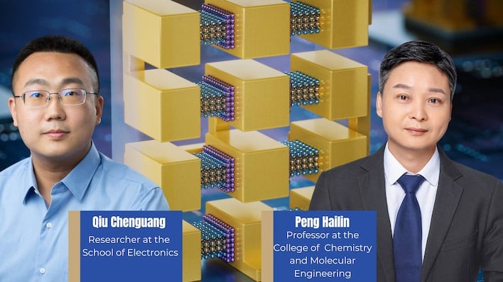
The Top 10 Semiconductor Stories of 2024: Trillion-transistor GPUs, steel-slicing laser chips, particle accelerators, and more
spectrum.ieee.org/top-semiconductor-stories-2024
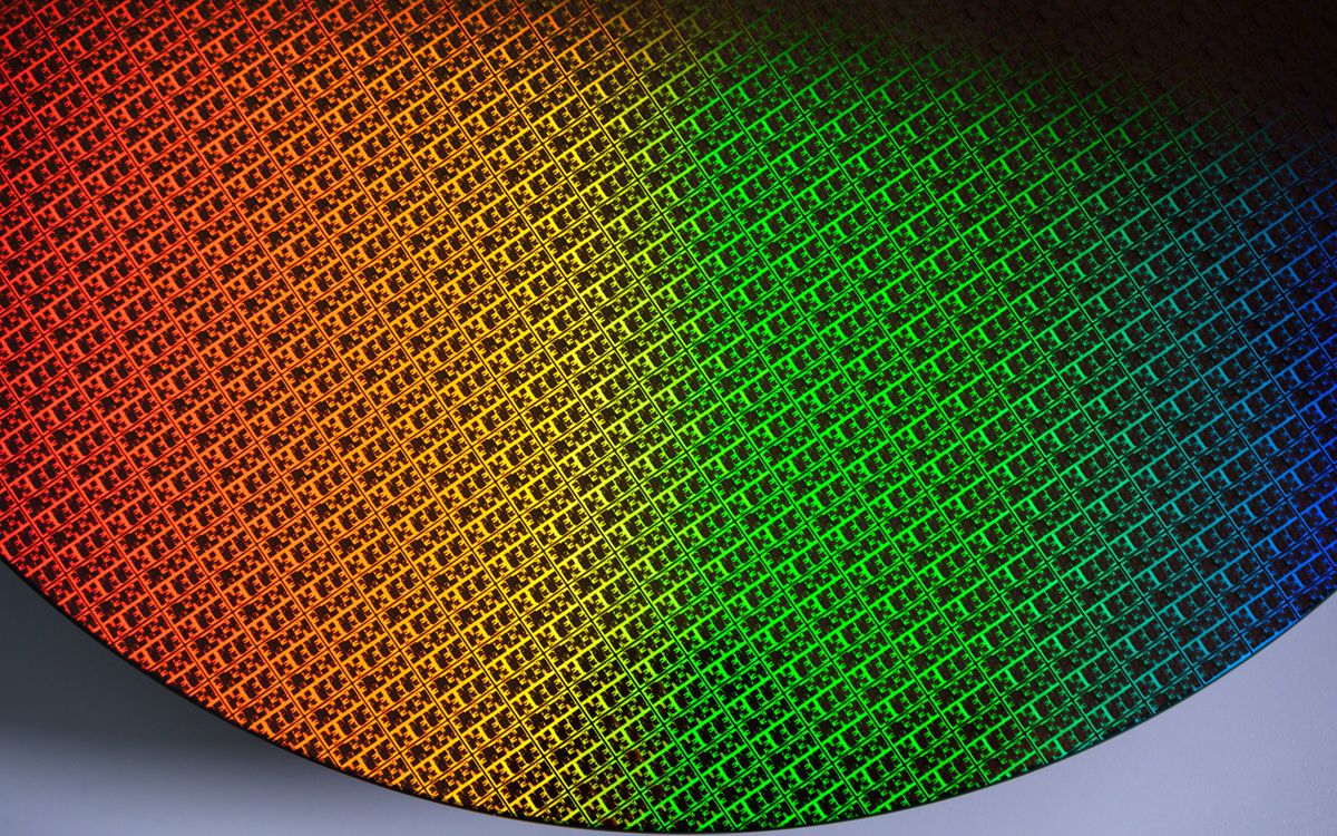
2D materials boost p-type transistor performance, paving way for future tech: After dominating the electronics industry for decades, conventional silicon-based ...
phys.org/news/2024-12-2d-materials-boost-p-transistor.html

TSMC Lifts the Curtain on Nanosheet Transistors: And Intel shows how far these devices could go
spectrum.ieee.org/tsmc-n2

Intel looks beyond silicon, outlines breakthroughs in atomically-thin 2D transistors, chip packaging, and interconnects at IEDM 2024
tomshardware.com/pc-components/cpus/intel-looks-beyond-silicon-outlines-breakthroughs-in-atomically-thin-2d-transistors-chip-packaging-and-interconnects-at-iedm-2024


The semiconductor industry faces its biggest technical challenge yet : As Moore’s law fades, how can more transistors be fitted onto a chip?
economist.com/technology-quarterly/2024/09/16/the-semiconductor-industry-faces-its-biggest-technical-challenge-yet

 Paid articlePaywall
Next