
Nature Jul 07
As transistors get smaller, electrodes must keep shrinking too:
Direct imaging shows that the contacts through which current flows into atomically thin ...
nature.com/articles/d41586-026-01807-y

Story Details
| Last Updated | |
| Total Articles | 2 |
Main Topics

Similar to This
Previous

Single 2D crystal transforms into transistor with built-in insulation and electrical contacts
phys.org/news/2026-10-2d-crystal-transistor-built-insulation.html


CXMT president says company’s first 4F² DRAM will be a server DDR5 RDIMM due by year-end — vertical transistors cut each memory cell’s footprint by a third on ...
tomshardware.com/pc-components/dram/cxmt-president-says-companys-first-4f2-dram-will-be-a-server-ddr5-rdimm-due-by-year-end-vertical-transistors-cut-each-memory-cells-footprint-by-a-third-on-paper-but-no-speeds-or-capacities-yet

 Paid articlePaywall
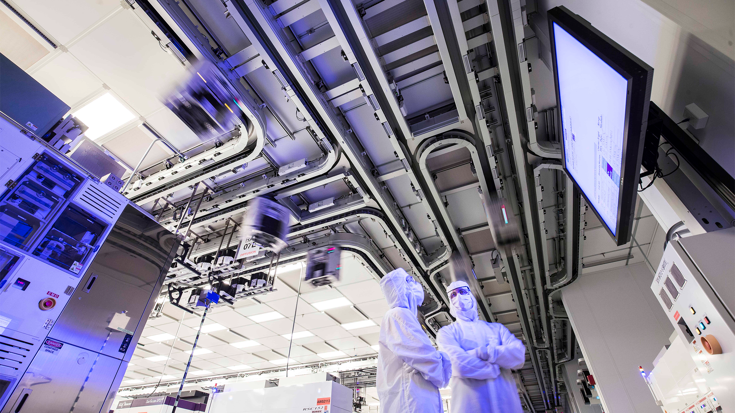
GlobalFoundries unveils 7nm-class FDX Fusion node — FD-SOI node doubles 22FDX transistor density, comes 7 years after firm abandoned FinFET
tomshardware.com/tech-industry/semiconductors/globalfoundries-unveils-7nm-class-fdx-fusion-node-fd-soi-node-doubles-22fdx-transistor-density-comes-7-years-after-firm-abandoned-finfet
 Paid articlePaywall

Wafer-Scale Superconducting Transistors Cut Cryo Cables: Startup S-Transistor says it can make superconducting transistors at scale
spectrum.ieee.org/superconducting-transistors

Atomically thin transistors could transform computing by surpassing silicon's switching limit
techxplore.com/news/2026-10-atomically-thin-transistors-surpassing-silicon.html


How 2nm technology improves iPhone performance: Discover how 2nm technology improves iPhone performance. Explore the A20 Pro chip, Gate-All-Around transistors ...
wionews.com/photos/how-2nm-technology-improves-iphone-performance-1789276386997

What TSMC's 2nm technology means for Apple: Discover what TSMC's 2nm technology means for Apple. Explore the N2 node exclusivity ...
wionews.com/photos/what-tsmc-s-2nm-technology-means-for-apple-1789647148778

'3nm technology': Why smaller chips are more powerful: Building 3-nanometre semiconductors allows manufacturers to pack 19 billion transistors onto a ...
wionews.com/photos/3nm-technology-why-smaller-chips-are-more-powerful-1785050135070

SMIC's third-gen 7nm node shows smaller metal pitch than Intel 18A, higher transistor density than TSMC N6 without EUV — analysis of N+3 shows significant ...
tomshardware.com/tech-industry/semiconductors/smics-third-gen-7nm-node-shows-smaller-metal-pitch-than-intel-18a-higher-transistor-density-than-tsmc-n6-without-euv-analysis-of-n-3-shows-significant-advancement-for-chinese-semi-manufacturin

techxplore.com Jun 26
Dog-bone design helps 2D nanoribbon transistors stay fast and efficient as widths shrink
techxplore.com/news/2026-06-dog-bone-2d-nanoribbon-transistors.html


Belgium's Imec partners with Taiwan's TSMC on transistor technology | Taiwan News | Jun. 16, 2026 18:36
taiwannews.com.tw/en/news/6383997

Atomic-level simulations predict transistor scaling limits: As the global semiconductor industry enters the so-called 2-nanometer process era ...
phys.org/news/2026-06-atomic-simulations-transistor-scaling-limits.html

matse.illinois.edu Jun 01
A new way to build chips: Sequentially stacking silicon to extend Moore’s law : Researchers led by Qing Cao have demonstrated a scalable way to directly and ...
matse.illinois.edu/news/85775


Huawei bets on speed over shrinking transistors to sidestep US chip sanctions: Huawei's new chip design principle focused on boosting transmission speed rather ...
reuters.com/world/china/huawei-bets-speed-over-shrinking-transistors-sidestep-us-chip-sanctions-2026-05-29/

Quantum Motion raises $160 million to build quantum computers from standard silicon transistors
reuters.com/technology/quantum-motion-raises-160-million-build-quantum-computers-standard-silicon-2026-05-07/


Inside the birthplace of your favourite technology: Many of our modern marvels are rooted in the legacy of Bell Labs, an innovation powerhouse in suburban New ...
thestar.com.my/tech/tech-news/2026/03/11/inside-the-birthplace-of-your-favourite-technology

Bill Gates-backed silicon photonics startup develops optical transistors 10,000x smaller than current tech — optical chip can process 1,000 x 1 ...
tomshardware.com/tech-industry/semiconductors/bill-gates-backed-silicon-photonics-startup-develops-optical-transistors-10-000x-smaller-than-current-tech-optical-chip-can-process-1-000-x-1-000-multiplication-matrices

Intel details progress on fabbing 2D transistors a few atoms thick in standard high volume fab production environment — chipmaker outlines 300-mm fab ...
tomshardware.com/tech-industry/semiconductors/intel-shows-300-mm-fab-compatible-integration-of-2d-transistor-contacts-and-gate-stacks


Electronics researchers have developed a new way to stack transistors in a die, to keep Moore's law alive for as long as possible
pcgamer.com/hardware/processors/electronics-researchers-have-developed-a-new-way-to-stack-transistors-in-a-die-to-keep-moores-law-alive-for-as-long-as-possible/

Next